- 您现在的位置:买卖IC网 > Sheet目录1219 > HIP6501AEVAL1 (Intersil)EVALUATION BOARD ACPI HIP6501
�� �
�
�Application� Note� 9846�
�State� Transition�
�Figure� 4� shows� the� transition� from� active� state� (S0,S1)� to� S3�
�sleep� state.� Prior� to� time� T0,� the� evaluation� board� was�
�operating� in� active� mode,� with� SW1� on� and� SW2� and� SW3�
�off.� At� time� T0,� SW2� is� switched� on,� triggering� the� switch-�
�over� of� the� output� regulation� from� the� active� ATX� output� rails�
�1� 4� >�
�3.3VIN�
�3.3V� DUAL�
�to� the� 5VSB� supply,� as� well� as� the� turn-off� of� the� ATX.� At�
�time� T1� the� ATX� responds� to� the� turn-off� request,� and� the� 5V�
�output� starts� to� ramp� down� under� the� current� draw� caused�
�by� the� embedded� 5� ?� serpentine� resistor.�
�5VIN�
�2� >�
�3>�
�5V� DUAL�
�2.5V� MEM�
�5V� DUAL�
�3.3V� DUAL�
�T0T1� T2�
�Ch1� 200mV� BW�
�Ch3� 200mV� BW�
�T3T4� T5�
�Ch2� 200mV� BW�
�Ch4� 200mV� BW�
�2.00ms� Ch4�
�3.19V�
�FIGURE� 5.� HIP6501AEVAL1� ACTIVE� STATE� (S0,S1)� OUTPUT�
�TRANSIENT� RESPONSE� (ALL� OUTPUTS�
�4� 123� >�
�2.5V� MEM�
�ENABLED)�
�Similar� explanation� accompanies� the� 5VDUAL� output�
�waveform,� except� that� the� ATX� 5V� output� could� not� be�
�shown� due� to� measurement� equipment� limitations.� However,�
�the� voltage� offset� caused� by� the� transient� load� application�
�T0�
�Ch1� 1.00V� BW�
�Ch3� 1.00V� BW�
�T1�
�Ch2� 1.00V� BW�
�Ch4� 1.00V� BW�
�2.00ms� Ch4�
�3.00V�
�can� be� identified� as� the� product� of� 50m� ?� and� 2.5A,� resulting�
�in� 125mV� of� voltage� droop.�
�The� situation� is� different� with� the� 2.5VMEM� output.�
�FIGURE� 4.� HIP6501AEVAL1� ACTIVE� STATE� (S0,S1)� TO�
�STANDBY� STATE� (S3)� TRANSITION� WITH� ALL�
�OUTPUTS� ENABLED�
�The� transition� back� from� S3� sleep� state� to� active� state�
�mirrors� the� active-to-sleep� state� transition,� above.�
�Transient� Response�
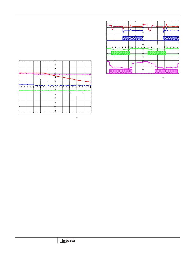
�In� Figure� 5,� all� the� outputs� of� the� evaluation� circuit� are�
�subjected� to� simultaneous� load� transients� while� operating� in�
�active� state� (S0,� S1).� Output� loading� of� each� output� consists�
�of� different� frequency� transients� of� amplitude� equal� to� the�
�maximum� active� state� current� as� defined� in� Table� 1,�
�superimposed� on� a� constant� 50mA� load.� The� output�
�transients’� rate� of� change� (dI/dt)� also� match� the� values�
�described� in� Table� 1.� All� outputs� shown� in� the� oscilloscope�
�capture� are� DC� offset� by� their� nominal� value,� and� all� are� DC�
�coupled.� The� rectangles� underneath� each� of� the� output�
�waveforms� indicate� the� duration� of� each� transient� occurring�
�on� the� respective� output.�
�As� it� can� be� seen� in� Figure� 5,� the� 3.3V� DUAL� output� follows�
�the� AC� meandering� of� the� ATX� 3.3V� output� very� accurately,�
�being� separated� only� by� the� r� DS(ON)� of� the� N-MOS� switch�
�(Q3A).� During� the� transient� loading,� the� 3.3VDUAL� output�
�develops� a� DC� offset,� due� to� the� voltage� droop� across� Q3A.�
�Specific� to� this� circuit� and� the� particular� circuit� loading,� the�
�offset� can� easily� be� identified� as� the� product� of� 50m� ?� and�
�3A,� resulting� in� 150mV� of� voltage� drop.�
�4�
�This� output� is� actively� regulated� by� the� IC,� and� the� resulting�
�output� regulation� is� a� combined� effect� of� high� dV/dt� ripple�
�caused� by� the� transient� edges,� decreased� voltage� overhead�
�for� the� pass� NPN� transistor� due� to� ATX� 3.3V� ripple,� as� well�
�as� DC� accuracy� of� the� internal� circuitry.� Under� the� combined�
�effects� of� all� parameters� listed� above� and� with� fairly� scarce�
�amounts� of� capacitance� present� on� board,� the� memory�
�output� is� still� maintained� within� a� 4%� tolerance.�
�Output� Short-Circuit� Protection�
�Figure� 6� depicts� the� circuit’s� behavior� in� response� to� a�
�sudden� output� short-circuit� (output� under-voltage),� applied� in�
�this� scope� capture� on� the� 2.5V� MEM� output,� while� operating�
�in� active� state.� At� time� T0� a� short-circuit� is� applied� using� an�
�electronic� load� -� as� a� result,� the� 2.5V� output� starts� to� rapidly�
�discharge,� crossing� the� falling� under-voltage� threshold� (68%�
�of� 2.5� =� 1.7V)� at� time� T1.� To� avoid� false� triggers,� the� UV�
�detector� is� equipped� with� a� 10� μ� s� filter.� As� the� UV� event�
�exceeds� the� 10� μ� s� window,� it� triggers� a� fault� response� at� time�
�T2.� The� logic� high� output� on� the� FAULT/MSEL� pin� sets� the�
�external� fault� latch� circuitry� which� quickly� discharges� the� SS�
�capacitor� just� below� the� chip� shutdown� level,� reached� at� time�
�T3.� The� chip� reset� disables� the� fault� reporting� and� the� latch�
�maintains� the� circuit� in� a� reset� state.� Depressing� the� CLEAR�
�FAULT� button� resets� the� latch� and� releases� the� circuit� for�
�operation.�
�发布紧急采购,3分钟左右您将得到回复。
相关PDF资料
HIP9011EVAL1Z
BOARD EVALUATION FOR HIP9011
HM2H08P115LF
HM2H08P115LF SHROUD STYLE B LF
HM2P12P1LF
HM2 M INS STYLE N WIDE
HM2R06P1LF
MILLIPACS RCP HSG
HM2SC22A8
HM2SC22A8-MILLIPACS 2R SHIELDING
HM2SC22B
HM2SC22B-MPACS SHIELD COVERS
HMC6352-DEMO
DEMONSTRATION BOARD FOR HMC6352
HMEG
FUSEHOLDER W/COVER FOR AMG FUSE
相关代理商/技术参数
HIP6501CB
制造商:Rochester Electronics LLC 功能描述:- Bulk
HIP6501CB-T
制造商:Rochester Electronics LLC 功能描述:- Tape and Reel
HIP6501EVAL1
制造商:INTERSIL 制造商全称:Intersil Corporation 功能描述:Triple Linear Power Controller with ACPI Control Interface
HIP6502
制造商:INTERSIL 制造商全称:Intersil Corporation 功能描述:Multiple Linear Power Controller with ACPI Control Interface
HIP6502 WAF
制造商:Intersil Corporation 功能描述:
HIP6502_00
制造商:INTERSIL 制造商全称:Intersil Corporation 功能描述:Multiple Linear Power Controller with ACPI Control Interface
HIP6502B
制造商:INTERSIL 制造商全称:Intersil Corporation 功能描述:Multiple Linear Power Controller with ACPI Control Interface
HIP6502BCB
制造商:Rochester Electronics LLC 功能描述:- Bulk